high-voltage-pulse-generator
Layout of Circuit
For the PCB design, it is recommended to follow these steps:
Layer Stack Manager {pagestep}
The thickness of each PCB layer is defined: solder mask, dielectric, and copper in top & bottom layer.
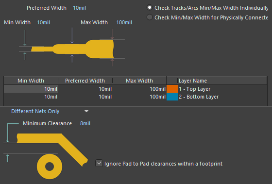
Design Rules {pagestep}
The width of the traces and their spacing are important parameters to define and affect the manufacturing capabilities. In our case, we manufacture the boards at PCBCart.
PCB routing {pagestep}
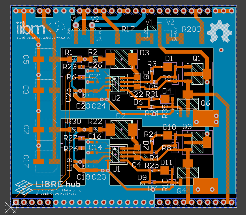
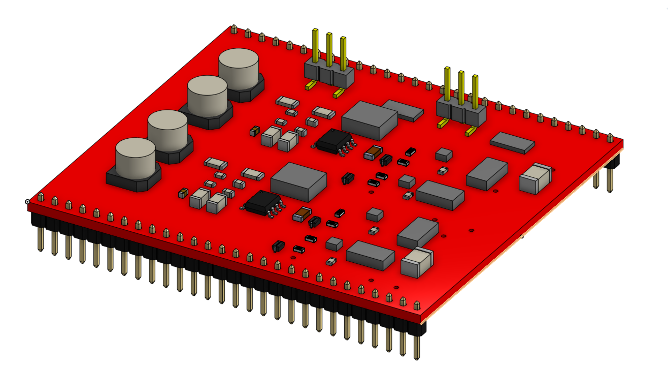
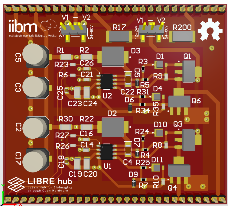
After defining the board shape and the origin, you can proceed to place the components in the active area (72x64mm) and start routing, taking care to any rule violations that may occur. You can view the 3D model of PCB here.
! Caution ! It is not recommended to use autoroute tool.


!! Warning !! !! Don’t try to connect V2 jumper from LT8361 because you may shortcircuit the high voltage to power ground. This could probably be solved by adding a snubber circuit in the MOSFETs of inverter circuit. Connect jumper in V1 in both headers and not change.
Gerber Files {pagestep}
Below are the Gerber files for you to attach and send to the PCB manufacturer.
i Note i In the CircuitMaker software, you can go to the Project section, select Generate Output Files, and then choose Gerber Files.

